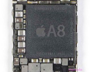
Apple A8 teardown reveals big processor power in small iPhone 6 package

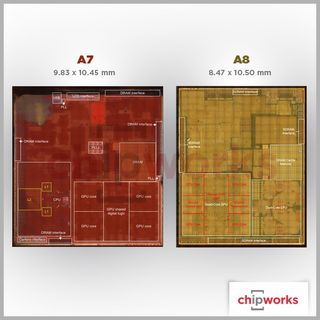
A teardown of the Apple A8 processor inside the iPhone 6 and iPhone 6 Plus reveals that Apple has indeed moved away from Samsung, fabbing their second-generation 64-bit system-on-a-chip on TMC's new 20nm process. That's what lets them get 2 billion transistors onto a package 15% smaller than the one that came before. They've also gone with a PowerVR GX6450 GPU and crammed 4 MB of L3 cache inside the application processor. All this, and more, according to Chipworks and expanded upon by AnandTech:
Overall, Chipworks' analysis points to A8 being fabbed on TSMC's 20nm process. This makes A8 among the first SoCs to receive the 20nm treatment. Thanks to this smaller node Apple has been able to build in additional features to the SoC while simultaneously shaving off around 15% of their die size. Chipworks estimates the final die size of A8 to stand at 89mm2, versus the 104mm2 for the Samsung 28nm based A7. Chipworks notes that if this were a straight shrink that one would expect the A8 to be closer to 50% the size of A7 (though not all logic can shrink quite that well), which indicates that Apple has spent quite a bit of die size on improving performance through more complex CPU and GPU architectures and miscellaneous feature additions.

All of this lines up with what Apple announced at the iPhone event earlier this month. Where the Apple A7 was about power and performance, the Apple A8 is about efficiency and battery life.
If you've got an iPhone 6 and iPhone 6 Plus, how's the Apple A8 been working for you?
Master your iPhone in minutes
iMore offers spot-on advice and guidance from our team of experts, with decades of Apple device experience to lean on. Learn more with iMore!
Most Popular


